-
-
-
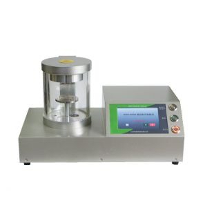
德國EBAC/RCI電子束吸收電流分析系統

- 品牌:德國博易
- 型號: EBAC/RCI
- 產地:歐洲 德國
- 供應商報價:¥150
-
尚豐科技(香港)有限公司
 更新時間:2023-04-10 10:05:46
 -
銷售范圍售全國
入駐年限第4年
營業執照已審核
- 同類產品應用(8件)

立即掃碼咨詢
聯系方式:400-822-6768
聯系我們時請說明在儀器網(www.ghhbs.com.cn)上看到的!
掃 碼 分 享 -
為您推薦
產品特點
- EBAC/RCI電子束吸收電流分析系統,能夠方便快速的定位半導體芯片電路中的短路及失效點位置,不但可以對同層電路,而且可以對次表層,甚至表層下第三層、第四層電路進行失效點的準確定位,因此能夠對半導體芯片電路或相關材料進行快速準確的失效分析。在保留掃描電鏡高分辨率的前提下,能夠對同層芯片電路進行高準確定位,同時能夠對次表層甚至表面下第三、第四層電路進行失效點定位
詳細介紹
尚豐科技向用戶提供專業的的電子束吸收電流分析系統EBAC/RCI
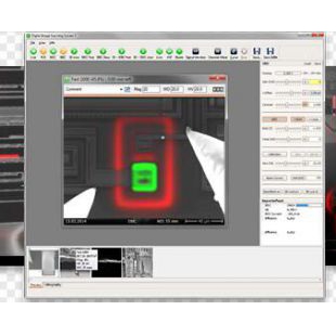
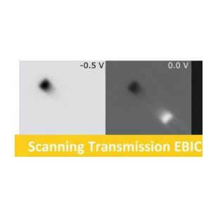
EBAC/RCI原理
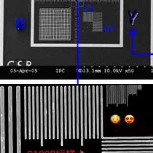
EBAC/RCI電子束吸收電流分析系統,能夠方便快速的定位半導體芯片電路中的短路及失效點位置,不但可以對同層電路,而且可以對次表層,甚至表層下第三層、第四層電路進行失效點的精確定位,因此能夠對半導體芯片電路或相關材料進行快速準確的失效分析。
目前,集成電路芯片設計越來越復雜,關鍵尺寸和金屬連線線寬越來越小,傳統的失效點定位方法,如微光顯微鏡或光束又到電阻變化鞥,由于其分辨率不足,導致不能精確地定位電路故障點位置,電壓襯度方法雖然在一些開路短路失效分析中能快速地定位失效點,但只是局限于電路同層分析。
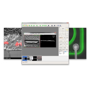
EBAC/RCI電子束吸收電流分析系統是基于掃描電鏡的分析系統,在保留掃描電鏡高分辨率的前提下,能夠對同層芯片電路進行高準確定位,同時能夠對次表層甚至表面下第三、第四層電路進行失效點定位,因此越來越多的應用于先進制程芯片的失效分析。在涉及多層金屬層的失效定位分析時,EBAC/RCI方法更加簡便精確,可保證分析的成功率,并縮短分析周期。EBAC/RCI acquisition
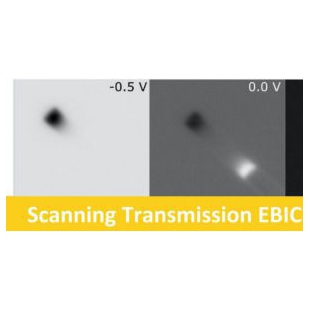
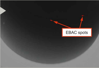
The lowest noise Electron Beam Absorbed Current (EBAC)
and Resistive Contrast Imaging (RCI)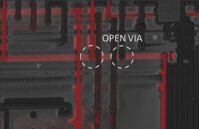
Find exact location of any open,resistive or shorting defect
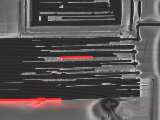
Localize metal line cuts caused by cracking,corrosion, electro-migration, or foreign particles
Identify resistive opens caused by interface contamination at via interconnects
Pinpoint location for direct TEM lamella FIB preparation
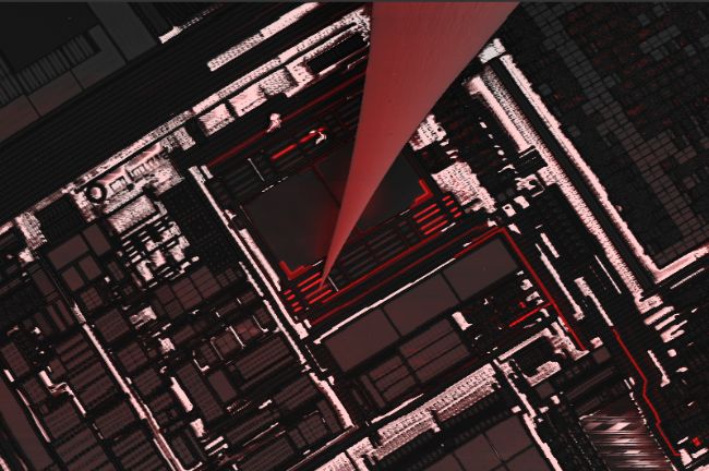 Characterize interconnects with highest resolution
Reveal electrical integrity of nets with sub-mciron lateral resolution and bridge from EFA to PFA
Diagnose fabrication and long term issues, including contamination,metal pattering defects, resistive interconnectors, or electro-migration
Directly isolate defects to the exact layer and die location, and improve them to product improvement actions
 Verify device operation modes with built-in biasing for voltage contrast
Image bias/voltage contrast in delayered devices
Monitor operation of devices under bias
Compare imaged behaviour with device design

Localize defects in thin dielectric layersVisualise and localise weaknesses in gate oxide (GOX) and capacitor oxide (COX) before breakdown
Pinpoint oxides shorts caused by ESD or EOS with sub-micron resolution
Preserve the original defect signature with power dissipation in the lower nW range during localization
Access failures invisible in voltage contrastFind low resistances that allow charge tunneling trough the interconnects
Investigate structures in contact with the silicon substrate
Characterize large metal structures
尚豐科技致力于引進推廣先進的材料、生物顯微觀測及微區分析儀器,向科研人員提供高附加值服務。
我們擁有一支涉及眾多領域高素質的應用支持團隊,為各行業的應用需求提供專業的解決方案和售后服務。
敬請聯絡